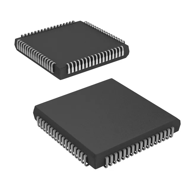
Infineon Technologies CY7C4245-15JXC — Memory (DRAM / SRAM / Flash / EEPROM)

CY7C4245-15JXC Synchronous FIFO, 66.7 MHz, 10 ns

MPNCY7C4245-15JXC
Obsolete

Infineon (Cypress) CY7C4245-15JXC synchronous FIFO, 66.7 MHz clock rate, 10 ns access time, 72K (4K x 18) memory, 4.5 V–5.5 V supply, 0°C–70°C, 68-PLCC (24.23x24.23 mm).

Independent supplier — new & surplus stockAuthenticity-screened · ESD-safe packingListing updated Jul 2026

Specifications

CY7C4245-15JXC specifications
ParameterValue
SeriesCY7C
MountingSurface Mount
Expansion typeDepth, Width
Supply voltage4.5 V ~ 5.5 V
Current - supply45mA
Operating temperature0°C ~ 70°C
PackageTray
FunctionSynchronous
Data rate66.7MHz
Access time10ns
Memory size72K (4K x 18)
FWFT supportNo
Case68-LCC (J-Lead)
Bus directionalUni-Directional
Retransmit capabilityYes
Programmable flags supportYes

Product details

The Infineon (Cypress) CY7C4245-15JXC is a synchronous FIFO memory with a 66.7 MHz clock rate and 10 ns access time, organised as 4K words by 18 bits (72K total).

66.7 MHz clock and 10 ns access — timing budget for the bus

The 66.7 MHz clock rate gives a 15 ns period. The 45 mA maximum supply current is a reasonable budget for a 5 V FIFO running at this speed; a 3.3 V-only system would need a level translator or a different FIFO family.

68-PLCC footprint — hand-solderable but board-hungry

The 68-PLCC (24.23 x 24.23 mm) J-lead package is one of the larger PLCC footprints.

Obsolete — no official successor on record

The CY7C4245-15JXC is listed as Obsolete. No official replacement part number is provided in the lifecycle record.

Frequently asked questions

Is CY7C4245-15JXC obsolete?

Yes, the CY7C4245-15JXC is listed as Obsolete. No official replacement part number is provided. For existing BOM lines, sourcing is through the surplus and broker channel.

What is the difference between CY7C4245-15JXC and CY7C4245-15JXI?

Both share the same 68-PLCC package, 66.7 MHz clock, and 10 ns access time.