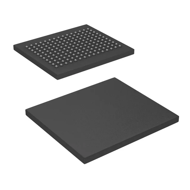
Infineon Technologies CY7C2665KV18-550BZXC — Memory (DRAM / SRAM / Flash / EEPROM)

Infineon CY7C2665KV18-550BZXC SRAM, 144Mbit, 550 MHz

MPNCY7C2665KV18-550BZXC
Active

Infineon CY7C2665KV18-550BZXC, QDR II+ synchronous SRAM, 144 Mbit (4M x 36), 550 MHz clock, parallel interface, 1.7V–1.9V supply, 165-FBGA (15x17 mm), 0°C to 70°C.

$356.6100Ref. price · indicative, final on quote
Independent supplier — new & surplus stockAuthenticity-screened · ESD-safe packingListing updated Aug 2026

Specifications

CY7C2665KV18-550BZXC specifications
ParameterValue
Memory typeVolatile
MountingSurface Mount
Supply voltage1.7V ~ 1.9V
Clock frequency550 MHz
Memory interfaceParallel
Operating temperature0°C ~ 70°C (TA)
PackageTray
TechnologySRAM - Synchronous, QDR II+
Memory size144Mbit
Memory formatSRAM
Case165-LBGA
Memory organization4M x 36

Product details

550 MHz QDR II+ SRAM for high-throughput buffer applications

Clock frequency and bus bandwidth — the 550 MHz edge

At 550 MHz, the CY7C2665KV18-550BZXC sustains a data rate of 1.1 G transfers per second per pin on a 36-bit-wide bus. That is roughly 22% higher throughput than the 450 MHz CY7C1650KV18-450BZC, which runs the same 4M x 36 organization at a lower clock. The trade-off is tighter timing closure on the PCB — the 1.8 ns cycle time leaves less margin for trace-length mismatch and requires controlled-impedance routing on all data and address lines.

The 165-ball FBGA (15x17 mm) uses a 1.0 mm ball pitch typical of high-density SRAM packages. The package has no exposed thermal pad — all heat dissipation is through the solder balls and the PCB copper planes. Place at least four 4.7 µF ceramic decoupling capacitors within 5 mm of the ball array on the 1.8 V supply rail to keep the transient response clean at 550 MHz switching.

It is not qualified for industrial or automotive temperature ranges — if the design sees -40°C or +85°C, look at the industrial-grade variants in the same family.

Frequently asked questions

What is the clock frequency of CY7C2665KV18-550BZXC?

The clock frequency is 550 MHz, supporting a peak data rate of 1.1 G transfers per second per pin on the 36-bit bus.

What is the equivalent part for CY7C2665KV18-550BZXC?

The CY7C1650KV18-450BZC is a functional peer with the same 144 Mbit density and 4M x 36 organization, but at a 450 MHz clock — a 100 MHz step down. For a higher-speed alternative, the CY7C2568XV18-633BZXC runs at 633 MHz but is organized as 4M x 18 (72 Mbit). Neither is a drop-in replacement; verify the bus width and speed grade against your design.