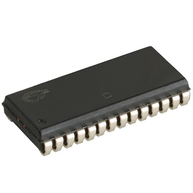
256 Kbit asynchronous SRAM for 5 V legacy buses
Housed in a 28-SOJ surface-mount package, this part is suited for high-speed cache, buffer memory, and microcontroller data storage in legacy 5 V digital systems where fast random access is required.
10 ns access time — timing closure for the bus
For a 33 MHz bus with a 30 ns cycle, this leaves 20 ns for address decode, setup, and hold — enough margin for most CPLD-based glue logic. If your system runs a 50 MHz bus (20 ns cycle), the 10 ns access consumes half the cycle, so check your timing budget against the address-to-data path.
5 V-only supply — not 3.3 V compatible
It is not designed for 3.3 V operation — driving the pins at 3.3 V logic levels will not guarantee correct read or write thresholds. If your system is 3.3 V, the CY7C1399BN-12VXI is a 3.0 V part in the same 32 K x 8 organization, though with a 12 ns access time. The 5 V rail also means the I/O levels are 5 V tolerant only; level translation is needed when interfacing with a 3.3 V controller.
Industrial temperature and 28-SOJ footprint
The 28-SOJ package has a 0.300-inch body width with J-bend leads on 1.27 mm pitch — a common footprint shared with many 28-pin SOJ SRAMs, so board layout reuse across density upgrades is straightforward. The part ships in Tube, which is typical for prototype and low-volume builds; for reel quantities, check the CY7C199D-10VXIT variant.
For production planning, the base part number CY7C199 spans multiple speed and temperature grades, so if a future speed or package change is needed, a pin-compatible variant within the family may be available without a board spin.