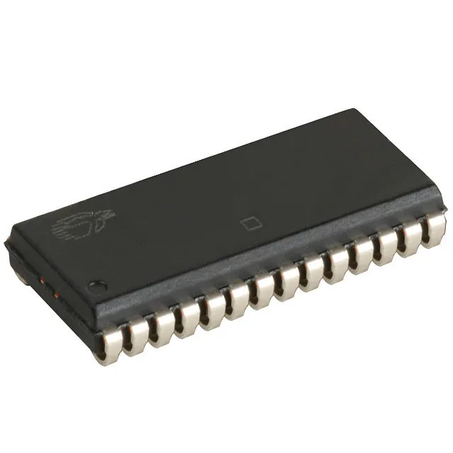
The CY7C199CN-12VXA: No franchised stock is claimed.
12 ns access — what it means for the bus
The 12 ns access time sets the minimum read-cycle window from address valid to data valid on the bus. For a 5V system running a 33 MHz bus (30 ns cycle), this SRAM leaves 18 ns of margin for address decode, board trace delay, and setup time at the controller — comfortable for most parallel interfaces. Write cycle time is also 12 ns (word, page mode), matching the read speed so the memory does not become the bottleneck in a balanced 32K x 8 memory map.
28-SOJ package — board-fit considerations
The J-lead footprint is compatible with legacy SOJ-28 layouts used across the CY7C199 family.