What this QDR II SRAM does in the system
Organized as 8M x 18, the 18-bit word width accommodates a 16-bit data payload plus two parity bits, a common requirement in networking packet buffers and telecom line-card lookup tables.
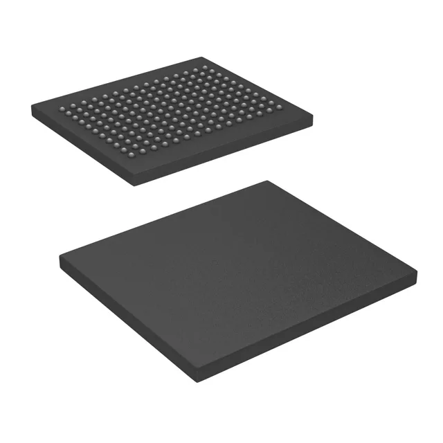
At 333 MHz the QDR II interface delivers a peak data rate of 666 million transfers per second per I/O pin (double data rate on both read and write ports). For a system designer this means the memory can keep up with a high-speed ASIC or FPGA memory controller without inserting wait states. The trade-off is that the 165-ball FBGA (15x17 mm body) demands careful signal-integrity layout — trace-length matching on the address and data busses, controlled impedance, and decoupling close to the supply balls.