The 300 MHz clock rate delivers a peak data bandwidth of 1.2 Gbps per I/O pin using the QDR II architecture, which dedicates separate read and write data ports to eliminate bus-turnaround dead cycles.
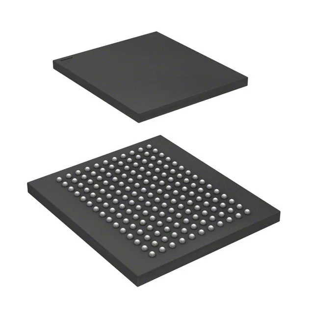
The 1.8V nominal rail is shared with many FPGA and ASIC core supplies, simplifying the power tree. Decoupling at the 165-FBGA (15x17) package should follow the manufacturer's recommended capacitor placement per the datasheet layout note — the fine-pitch BGA balls (0.8 mm pitch typical for this footprint) mean the VDD and VSS ball map dictates the via pattern and plane stitching.
The base product number CY7C1612 covers a family of density and speed variants; the -300BZXI suffix selects the 300 MHz speed grade in the 165-FBGA package with industrial temperature range.