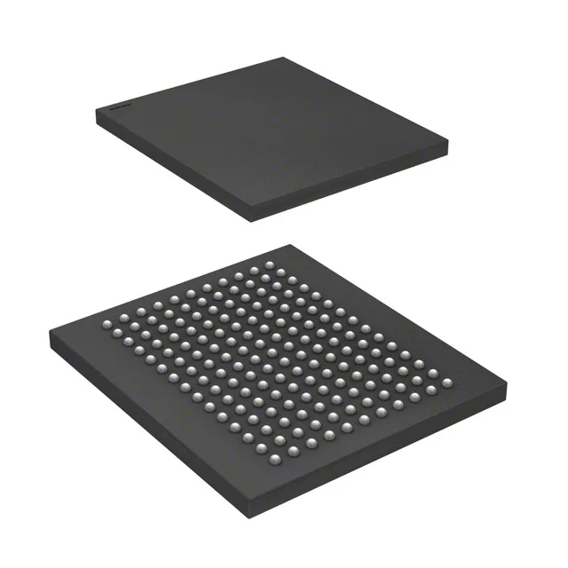
250 MHz DDR II SRAM for high-throughput designs
The CY7C1523AV18-250BZC is a 72 Mbit synchronous DDR II SRAM organized as 4M x 18 bits. It operates at a 250 MHz clock rate using a double-data-rate interface.
What the 250 MHz clock and DDR II interface mean for your bus
The 250 MHz clock rate with DDR II signalling means the SRAM delivers data at 500 million transfers per second on the 18-bit data bus. For a design that needs to sustain a 9 Gbps read/write pipeline (18 bits × 500 MT/s), this part keeps the bus margin tight. The DDR II architecture eliminates dead cycles between read and write turns, which is critical when the memory is shared between a processor and a DMA engine. The parallel interface at these speeds demands careful PCB layout — the 165-ball FBGA with a 1.0 mm ball pitch requires matched trace lengths and controlled impedance on the data and address lines. The 1.7 V–1.9 V supply rail also needs a clean, low-noise regulator; a 1.8 V LDO with ceramic output caps is the typical pairing.