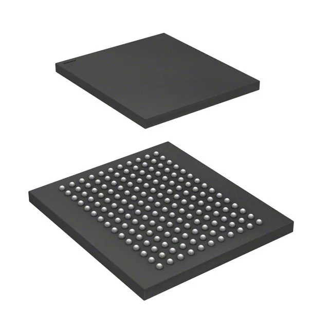
The CY7C1520AV18-250BZXC: This gives the system a high-bandwidth memory interface for applications that need deterministic, low-latency access — typically network packet buffers, telecom line cards, test equipment, and high-end FPGA-based processing where the bus must sustain back-to-back reads and writes without dead cycles.
250 MHz clock — timing margin and bus design
At 250 MHz the DDR II interface transfers data on both clock edges. The 2M x 36 organization moves 36 bits per edge.
Infineon (formerly Cypress) has ended production of this specific variant. The 165-LBGA package and the commercial temperature grade narrow the available pool, so lead times and pricing are quoted per lot against an RFQ. Any buyer sourcing this part should confirm date code, moisture sensitivity level (MSL), and traceability with the supplier.