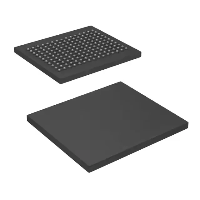
72 Mbit QDR II SRAM for high-throughput line cards
It clocks at 167 MHz and uses a parallel interface, giving it the read-write bandwidth needed for packet buffers, lookup tables, and traffic managers in networking and telecom equipment.
167 MHz clock and 2M x 36 organization — what they mean for throughput
The 167 MHz clock rate, combined with the QDR II architecture's separate read and write ports, delivers a peak data rate of 12 Gbps (167 MHz x 36 bits x 2 ports). That throughput is what makes this part a fit for high-port-count switches and routers where the SRAM must keep up with the line rate without stalling the pipeline. The 2M x 36 organization also aligns naturally with 36-bit-wide data buses common in network processors and FPGAs, avoiding the need for multiple narrower memories.
165-ball FBGA — layout and assembly notes
The part comes in a 165-ball LBGA (15x17 mm FBGA footprint). That is a fine-pitch BGA — not a hand-solderable package. The board needs a controlled reflow profile, X-ray inspection for voiding, and careful decoupling placement close to the supply balls. The 1.7V to 1.9V core supply is tight; a local LDO or low-noise regulator per the datasheet's recommended decoupling scheme keeps the SRAM's internal PLL clean.