Organized as 4M words by 18 bits, it runs at a 200 MHz clock frequency, giving a peak data rate that suits high-bandwidth buffer applications like network switch packet memory, test equipment waveform storage, or any system that needs low-latency, high-throughput SRAM without the dead cycles of traditional asynchronous parts.
At 200 MHz the QDR II interface delivers two independent read and two independent write data transfers per cycle, so the effective data rate is four times the clock frequency on each 18-bit port. That eliminates the bus-turnaround penalty you get with common-I/O DDR SRAMs; back-to-back reads and writes happen without idle cycles. The trade-off is a more complex controller — you need a QDR II memory controller that manages separate read and write data buses, typically built into a high-end FPGA or ASIC.
Supply and temperature — the design constraints
The PCB needs a clean 1.8 V rail with less than 50 mV ripple; a separate LDO for the SRAM supply is common. If the system sees -40°C or +85°C ambient, this SRAM is out of the running.
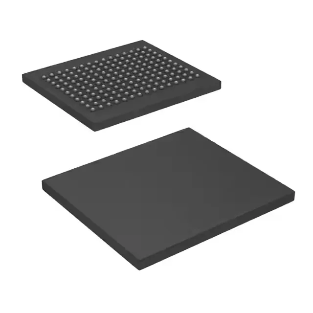
Housed in a 165-ball LBGA (fine-pitch BGA) measuring 15 mm x 17 mm. Surface-mount only, no socket-friendly variant. The ball pitch is 1.0 mm; via-in-pad or microvia fanout is typically needed for the inner rows. The package is compatible with other Cypress QDR II SRAMs in the same density and speed grade, which matters if you need to swap speed bins without a board spin.
Lifecycle reality — obsolete, no official successor
That means no last-time-buy window to catch; the factory has stopped production. Any stock on the open market is from surplus, overstock, or broker channels. The 165-ball FBGA footprint and QDR II interface are not directly drop-in replaceable with a current-production Infineon SRAM — a redesign would be needed to move to a newer family like QDR IV or RLDRAM.
Sourcing posture
If you have a production line that still uses this part, let us know the quantity and target date code; we can search our network for matching stock.