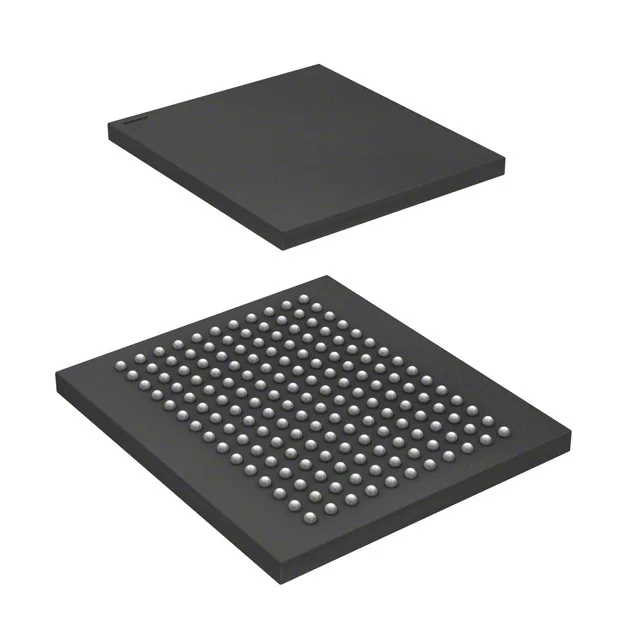
The CY7C1512V18-200BZXC: QDR II (Quad Data Rate) separates read and data buses so the memory can transfer data on both clock edges on each bus simultaneously, effectively quadrupling the throughput of a conventional single-data-rate SRAM at the same clock frequency. The 200 MHz clock rate gives this part a peak bandwidth suitable for high-throughput buffer applications in networking switches, routers, and telecom line cards where back-to-back read-write operations with no dead cycles are required.
Obsolete — plan for last-time-buy or alternative sourcing
Any replacement would require evaluating the broader QDR II / QDR IV family for footprint, supply voltage, and timing compatibility.
Package and footprint — 165-ball FBGA, 15 x 17 mm
Supplied in a 165-ball LBGA (supplier device package 165-FBGA, 15 x 17 mm body), surface-mount only. The tray shipping medium is standard for this BGA package.