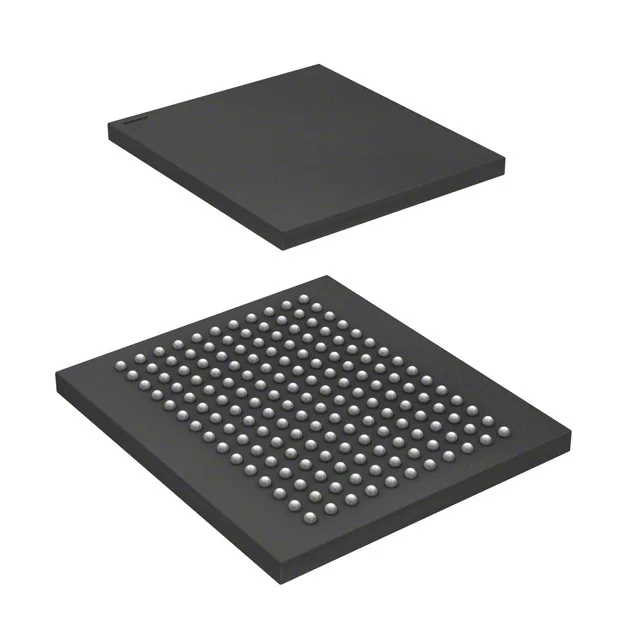
It clocks at 250 MHz on a parallel interface, delivering separate read and write ports that eliminate bus-turnaround dead cycles — a key advantage over standard synchronous SRAM for high-throughput applications.
250 MHz clock and QDR II bus — what the rating means for the design
At 250 MHz the QDR II architecture delivers two data transfers per clock cycle on separate read and write ports, so the effective data rate per pin is 500 Mbps. For a 72 Mbit device organized 4M x 18, the aggregate bandwidth reaches 9 Gbps on the read port and 9 Gbps on the write port simultaneously. That sustained throughput matters when the SRAM sits between a high-speed ASIC or FPGA and a lookup table or buffer — the bus never stalls waiting for read/write direction changes.