QDR II SRAM at 167 MHz — what this part does
The CY7C1512AV18-167BZXI: QDR II separates the read and write data buses so the controller can issue a read and a write on every clock edge without bus-turnaround dead cycles — a throughput advantage over common DDR or NoBL SRAMs in the same density class. The 167 MHz clock rate means the part delivers back-to-back data at 334 million transfers per second on each bus.
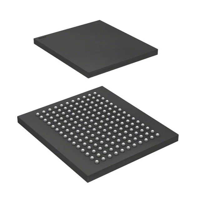
Housed in a 165-ball FBGA measuring 15 by 17 mm (supplier device package 165-FBGA). The ball pitch is 1.0 mm, which is a common BGA pitch for high-density memory — the PCB needs via-in-pad or microvia routing if you're bringing out all 18 data bits plus address on an inner layer.
Obsolete — sourcing reality now
Cypress (now Infineon) lists the CY7C1512AV18-167BZXI as obsolete. The last-time-buy window has closed — this part is no longer orderable through the factory or authorized distribution. Date codes will vary and may be several years old. Counterfeit risk is real for any obsolete high-value SRAM — insist on source inspection or X-ray verification before accepting delivery.