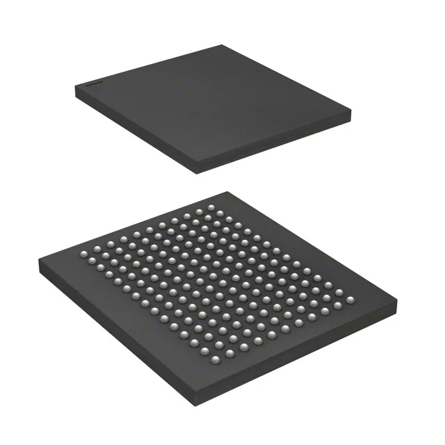
Infineon Technologies CY7C1484BV33-250BZXC — Memory (DRAM / SRAM / Flash / EEPROM)

CY7C1484BV33-250BZXC SRAM, 72Mbit, 250 MHz, 3 ns Access

MPNCY7C1484BV33-250BZXC
Obsolete

Infineon CY7C1484BV33-250BZXC synchronous SRAM, 72Mbit (2M x 36), 250 MHz clock frequency, 3 ns access time, parallel interface, 3.135V–3.6V supply, 0°C–70°C, 165-LBGA (15x17 mm FBGA).

$165.8900Ref. price · indicative, final on quote
Independent supplier — new & surplus stockAuthenticity-screened · ESD-safe packingListing updated Jul 2026

Specifications

CY7C1484BV33-250BZXC specifications
ParameterValue
Memory typeVolatile
MountingSurface Mount
Supply voltage3.135V ~ 3.6V
Clock frequency250 MHz
Memory interfaceParallel
Operating temperature0°C ~ 70°C (TA)
PackageTube
TechnologySRAM - Synchronous, SDR
Access time3 ns
Memory size72Mbit
Memory formatSRAM
Case165-LBGA
Memory organization2M x 36

Product details

Infineon lists the CY7C1484BV33-250BZXC as obsolete. That means no factory orders, no last-time-buy window — the only channel is independent distribution sourcing surplus inventory. Any production-run or repair BOM that carries this line needs a replacement qualified before stock dries up.

250 MHz clock, 3 ns access — what it buys you

This is a synchronous SDR (single-data-rate) SRAM clocked at 250 MHz, with a 3 ns access time from clock edge. The 72Mbit density is organized 2M x 36 — a 36-bit wide word that suits processor or FPGA cache lines without external muxing. Supply runs 3.135V to 3.6V, so it drops into a 3.3V nominal rail with margin for ripple. The 165-LBGA (15x17 mm FBGA) footprint is a fine-pitch BGA; route the 36 data lines plus address and control with matched length if you're pushing the 250 MHz edge.

Frequently asked questions

Is CY7C1484BV33-250BZXC obsolete?

Yes, Infineon has marked the CY7C1484BV33-250BZXC as obsolete. There is no active factory production — supply is limited to surplus and broker inventory.

What is the access time of CY7C1484BV33-250BZXC?

The access time is 3 ns from the clock edge, at the rated 250 MHz clock frequency. This is the time from the rising clock edge to valid data on the output pins — critical for zero-wait-state cache or high-speed buffer designs.