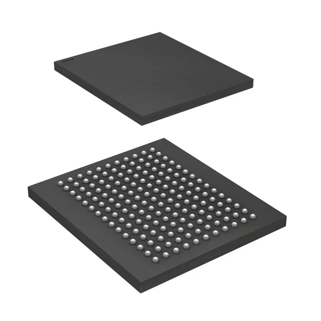
72Mbit synchronous SRAM in a 165-ball BGA
The CY7C1481BV33-133BZI: The 36-bit-wide datapath maps directly to 32-bit or 36-bit memory buses without external muxing — common in network processors, baseband ASICs, and high-end FPGA designs that need a wide, fast scratchpad. Packaged in a 165-ball FBGA (15x17 mm), it is a fine-pitch BGA requiring controlled reflow and X-ray inspection for void-free solder joints.
Supply and timing margins for the BOM
Supply voltage spans 3.135V to 3.6V — a 3.3V nominal rail with ±5% tolerance covers the full operating envelope. The parallel memory interface uses a standard synchronous protocol (SDR) — no DDR strobe or source-synchronous clocking, so the board layout is simpler than a DDR SRAM but throughput is limited to one data transfer per clock edge. For a 133 MHz bus, peak bandwidth is 133 MT/s per pin, or 4.8 GB/s across the 36-bit data bus.
Obsolete — sourcing through independent channels
Sourcing is per-RFQ — each lot is verified for authenticity, date code, and condition before shipment. No pin-compatible drop-in replacement from Infineon has been published; a board-level redesign may be required if a functional equivalent is needed.