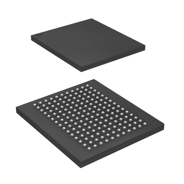
72Mbit synchronous SRAM at 250 MHz
The CY7C1480BV33-250BZI is a 72Mbit synchronous SRAM organized as 2M x 36, clocked at 250 MHz with a 3 ns access time — a fit for high-throughput FPGA block RAM expansion or packet buffer designs where the bus must run at the core clock rate without wait states. Supply range is 3.135V to 3.6V, so it sits on a 3.3V rail with margin for ripple — no separate VIO or VDDQ plane needed.
Industrial temperature and FBGA footprint
Housed in a 165-ball FBGA measuring 15x17 mm, the 1.0 mm ball pitch requires a 4-layer PCB minimum for signal fan-out — the inner layers carry the VDD and VSS planes that keep the supply impedance under 1 ohm at 250 MHz.