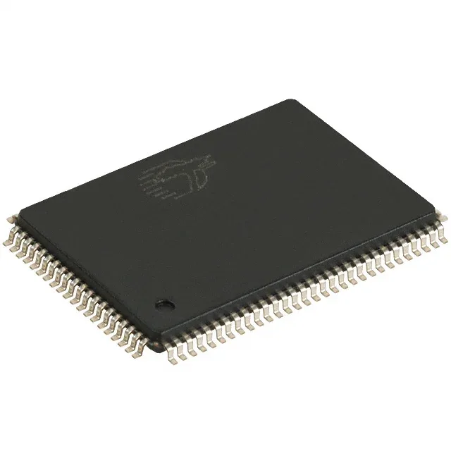
72 Mbit synchronous SRAM for high-throughput data paths
It uses a parallel memory interface and operates from a 3.135V to 3.6V supply, nominally 3.3V.
The 200 MHz clock frequency and 3 ns access time are the headline ratings that determine whether this part meets your read-cycle timing budget. At 200 MHz the clock period is 5 ns, so a 3 ns access leaves 2 ns for address hold, data setup, and board-level flight time. That is tight but workable with proper signal-integrity layout — keep the clock trace unterminated below 50 mm and match the data-bus lengths within 10 mm. The 3 ns access is the parameter to verify against your FPGA or ASIC's input setup requirement; if your controller needs 3.5 ns or more, you will need a slower speed grade or a pipelined (NoBL) architecture.
2M x 36 organization — why 36 bits?
The 2M x 36 organization is not arbitrary — 36-bit wide words map directly to common data-bus widths in high-end networking and telecom designs: 32-bit data plus 4-bit parity or ECC. If your system uses a 32-bit bus with byte parity, this part provides the extra four bits without needing a second device. For a 64-bit data path you would pair two of these, sharing the address and control lines. The 72 Mbit density (2M locations x 36 bits) also suits deep FIFO or large look-up tables where 64 Mbit or 128 Mbit parts are overkill.
Commercial temperature grade — indoor equipment only
That is the commercial grade, which limits this part to indoor, controlled-environment equipment — office networking, telecom central office, test equipment, and server-class hardware. Do not use this in outdoor base stations, automotive, or industrial enclosures where ambient can exceed 70°C or dip below freezing. For extended temperature (-40°C to 85°C or 105°C) you would need the industrial-grade variant in this family, which carries a different suffix.