72 Mbit synchronous SRAM with 200 MHz pipeline — the high-throughput buffer choice
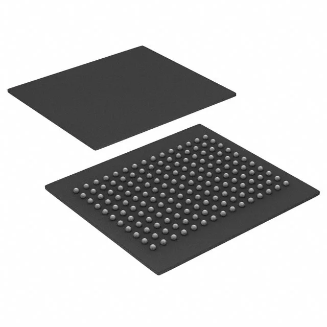
It operates from a 2.375V to 2.625V supply and is housed in a 165-ball FBGA (15x17 mm). This part is designed for high-bandwidth applications such as network packet buffers, telecom line cards, test equipment, and FPGA co-processing where deterministic latency and full-speed read/write cycles are required without the refresh overhead of DRAM.
200 MHz clock and 3 ns access — what they mean for timing closure
The 200 MHz clock frequency sets the maximum throughput at 200 million transfers per second on a 36-bit bus. The 3 ns access time is the window from clock edge to valid data out; at these speeds, board-level trace length matching and signal termination become critical. Expect to budget for controlled-impedance routing on all data and address lines, and place the SRAM close to the controller to minimize flight time. The 2.5V supply range (2.375V to 2.625V) aligns with JEDEC standard 2.5V I/O, so level translation is needed if the host uses 1.8V or 3.3V logic.
Last-time-buy — the sourcing window is closing
This means the manufacturer has announced end-of-life and is accepting final orders for a limited period. Once the last-time-buy window closes, the part will no longer be available through official distribution channels. For production builds that depend on this exact density and package, the procurement decision is time-sensitive: secure inventory now or qualify an alternative before the window shuts.