Clock rate and access time — bus timing margin
The CY7C1474V33-167BGC: The access time is the window from the clock edge to valid data on the bus — the memory controller's input setup/hold must fit within this window, and the 3.4 ns figure sets the upper bound for the read data capture timing at speed.
Density and organization — wide data path
72 Mbit density organized as 1M x 72 — a 72-bit wide data bus that matches the width of a 64-bit processor bus plus ECC byte lane without external muxing. The NoBL (No Bus Latency) architecture eliminates dead cycles between read and write operations, sustaining full pipeline throughput.
Package and supply — layout constraints
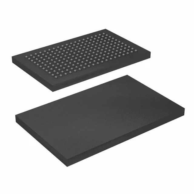
Housed in a 209-ball FBGA (14x22 mm) — the 0.80 mm ball pitch requires a four-layer PCB minimum for fan-out of the 72 data lines plus address and control.
Temperature grade — deployment envelope
This limits deployment to controlled indoor environments — telecom central office, data-center line cards, or benchtop instrumentation. Not qualified for extended industrial or automotive ambient ranges; a thermal chamber sweep should verify the timing margins at the upper temperature corner.