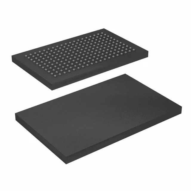
72 Mbit synchronous SRAM for high-throughput data planes
The CY7C1474V25-200BGI is a 72 Mbit synchronous SRAM from the NoBL (No Bus Latency) family, organized as 1M x 72 and clocked at 200 MHz. The 3 ns access time means the first read word appears on the bus within three clock edges after the address is presented — critical for zero-wait-state cache or packet-buffer lookups where every cycle counts. The 72-bit wide data bus maps naturally to 64-bit data paths with parity or ECC bits, so a single chip serves the full memory width of a network processor or FPGA without ganging multiple narrower parts.
Last Buy — what it means for procurement
Infineon has classified this part as Last Buy — the final production window is open, and once the inventory is exhausted the manufacturer will not replenish. This is the trigger to secure lifetime-buy quantities or qualify a replacement before the allocation dries up.
Industrial temperature grade and 2.5 V supply rail
The supply tolerance is tight — 2.375 V to 2.625 V — so the 2.5 V rail must stay within ±2.5 % including ripple; a standard 2.5 V LDO with 1 % accuracy covers this comfortably. The 209-ball FBGA package (14 x 22 mm body) uses a 1.0 mm ball pitch. Page 7 of the datasheet (the mechanical drawing) shows the ball map — the outer two rows are mostly VDDQ and VSS, which simplifies fan-out on a 6-layer PCB; the core signals sit in the inner rows.
NoBL architecture — why it matters for throughput
The NoBL (No Bus Latency) pipeline eliminates the dead cycle between consecutive read and write operations that plagues standard synchronous SRAMs. On a back-to-back read-after-write sequence, the data appears on the bus without inserting an idle clock — this lifts sustained throughput to near the clock rate for mixed-transaction traffic. The parallel memory interface (address, data, control) is JEDEC-compatible with other 1M x 72 pipelined SRAMs, so the PCB layout and FPGA controller logic can be designed to accept multiple second-source candidates from the same socket.