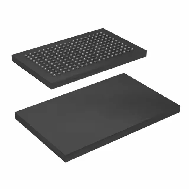
Infineon Technologies CY7C1474BV33-200BGXC — Memory (DRAM / SRAM / Flash / EEPROM)

CY7C1474BV33-200BGXC Infineon NoBL SRAM, 72Mbit, 200 MHz

MPNCY7C1474BV33-200BGXC
Active

Infineon Technologies NoBL™ synchronous SRAM, CY7C1474BV33-200BGXC, 72Mbit, 1M x 72, 200 MHz clock, 3 ns access, 209-FBGA (14x22 mm), 3.3V supply, commercial temp.

$172.4800Ref. price · indicative, final on quote
Independent supplier — new & surplus stockAuthenticity-screened · ESD-safe packingListing updated Aug 2026

Specifications

CY7C1474BV33-200BGXC specifications
ParameterValue
SeriesNoBL™
Memory typeVolatile
MountingSurface Mount
Supply voltage3.135V ~ 3.6V
Clock frequency200 MHz
Memory interfaceParallel
Operating temperature0°C~70°C(TA)
PackageTray
TechnologySRAM - Synchronous, SDR
Access time3 ns
Memory size72Mbit
Memory formatSRAM
Case209-BGA
Memory organization1M x 72

Product details

NoBL pipeline — why the dead cycle disappears

The CY7C1474BV33-200BGXC is a 72 Mbit synchronous SRAM from Infineon's NoBL™ (No Bus Latency) family, organized 1M x 72. The NoBL pipeline lets the memory accept a new read or write address on every clock cycle without inserting a dead cycle between read-to-write or write-to-read transitions — the bus stays full at 200 MHz. For a system architect sizing the memory bus, the 200 MHz clock rate sets the peak bandwidth at 1.6 GB/s (200 MHz × 72 bits ÷ 8). The 3 ns access time from address to valid data means the first read latency is three cycles; after that, the pipeline delivers one 72-bit word per clock.

The commercial temperature grade (0 °C to 70 °C) limits this part to indoor, climate-controlled environments — no extended temp for telecom cabinets or outdoor base stations. The 209-ball FBGA (14 mm × 22 mm) uses a 1.0 mm ball pitch. A pcb_layout_engineer should budget four signal layers for fan-out; the inner balls on a 14×22 array require microvias or buried vias in a standard 8-layer stack-up.

Active lifecycle — no end-of-life pressure

Infineon lists the CY7C1474BV33-200BGXC as Active (current production). The base product number CY7C1474 covers multiple speed grades and temperature ranges; the -200BGXC suffix identifies the 200 MHz, commercial-temp, 209-FBGA variant in tray packaging.

Frequently asked questions

What does the NoBL™ series mean for this SRAM?

NoBL (No Bus Latency) eliminates the dead cycle between read and write operations. The pipeline accepts a new address every clock cycle regardless of the previous operation, so the bus runs at full 200 MHz throughput without idle cycles.

What is the memory organization and interface of CY7C1474BV33-200BGXC?

It is organized 1M x 72 bits (72 Mbit total) with a parallel synchronous interface. The 72-bit data bus is suited for wide-word applications like network switch buffers or cache memory where a single access delivers a full cache line.

What package does this part use, and what are the board-level considerations?

The BGA footprint requires careful fan-out planning — inner rows typically need microvias or buried vias in a multi-layer PCB.