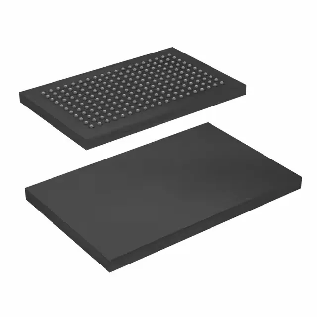
72Mbit NoBL synchronous SRAM — now obsolete
The Infineon (formerly Cypress) CY7C1474BV33-200BGI is a 72Mbit synchronous SRAM from the NoBL™ (No Bus Latency) family, organized 1M x 72 with a 200 MHz clock and 3 ns access time.
The 200 MHz clock rate and 3 ns access time are the headline numbers that define this part's position in the synchronous SRAM market. At 200 MHz, the memory delivers a 5 ns cycle time, and the 3 ns access means the first data word appears on the bus within three clock edges of the address being latched. The NoBL architecture eliminates the dead cycles that traditional pipelined SRAMs insert between read and write turns — back-to-back transactions run at full clock rate with no bubble. For a 64-bit system running at 200 MHz, that translates to a sustained throughput of 1.6 GB/s on a single chip, which is the kind of bandwidth a high-end packet processor or FPGA-based frame buffer needs to avoid stalling. The 3 ns access time also sets the timing closure budget for the FPGA or ASIC interface. With a 5 ns cycle, the 3 ns access leaves 2 ns for PCB trace delay, clock skew, and setup time at the controller — tight but achievable with controlled-impedance routing and matched-length traces on the 72-bit data bus. The 209-FBGA package (14x22 mm) keeps the signal paths short, but the BGA fanout requires at least a four-layer PCB to route all 72 data lines plus address and control cleanly.
The 3.135V to 3.6V supply range covers a nominal 3.3V rail with ±5% tolerance, which is the standard for most mid-range FPGA and ASIC banks. If your system runs a 3.3V rail that dips to 3.0V during a brownout, this part will not hold data — the minimum is 3.135V, so a separate supervisor or hold-up capacitor is needed.