The NoBL architecture eliminates the dead bus cycle between read and write operations, allowing back-to-back transactions at the full 167 MHz clock rate with a 3.4 ns access time.
At 167 MHz the cycle time is 6 ns. The 3.4 ns access time leaves roughly 2.6 ns of setup-and-hold budget for the FPGA or ASIC on the other side of the bus — enough for most 2.5 V interfaces without external PLL retiming, but tight enough that trace-length matching on the 72-bit data path matters. This part was designed into systems that cannot tolerate the dead cycle of a standard pipelined SRAM; the NoBL flow-through lets the controller issue a read on one clock edge and a write on the next without an idle cycle.
No direct successor order code is provided in the lifecycle record. If a form-fit-function replacement is needed, Infineon's broader NoBL and synchronous SRAM portfolio includes pin-compatible density and speed grades, but the exact 1M x 72 organization at 167 MHz in a 209-FBGA should be validated against the current product selector.
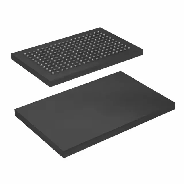
209-ball FBGA — footprint and handling
The 1.0 mm ball pitch is standard for this density, but the 14x22 mm body is longer than the more common 13x18 mm 209-ball footprint — verify the PCB land pattern against the supplier device package drawing. The Tray shipping medium means the parts are not on tape; plan for pick-and-place with a tray feeder or transfer to tape at the CM.