NoBL pipeline — why the dead bus cycle disappears
The CY7C1472V33-200AXC is a 72 Mbit synchronous SRAM from Infineon's NoBL (No Bus Latency) family, organized 4 M x 18. The NoBL pipeline lets the memory accept a new read or write address on every clock edge without inserting idle cycles between bus-turn operations — a standard synchronous SRAM stalls one cycle when switching from read to write, but this part keeps the bus full at 200 MHz. That 200 MHz clock rate, combined with the 3 ns access time, delivers a peak random-access bandwidth of 400 MB/s on a 32-bit data bus (or 450 MB/s on the native 18-bit word). The 3 ns figure is the first-word latency from address assertion to data valid; subsequent words in a burst follow at the clock rate.
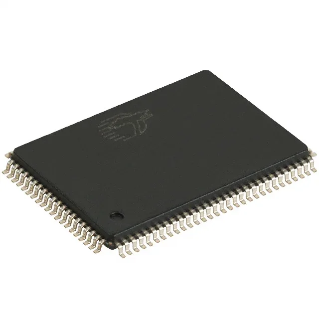
A switching regulator feeding this SRAM should stay within 3.3 V ± 0.165 V at the device pins; a linear regulator with 200 mV dropout is marginal if the input rail is 3.3 V. This part is specified for indoor equipment — telecom central-office switches, base-station line cards, network routers, and test equipment — not for outdoor or under-hood deployment. The 100-TQFP package (14 x 20 mm, 0.5 mm pitch) requires a 4-layer PCB for fan-out of the inner rows; the exposed pad is not present on this package, so thermal relief is through the leads alone.