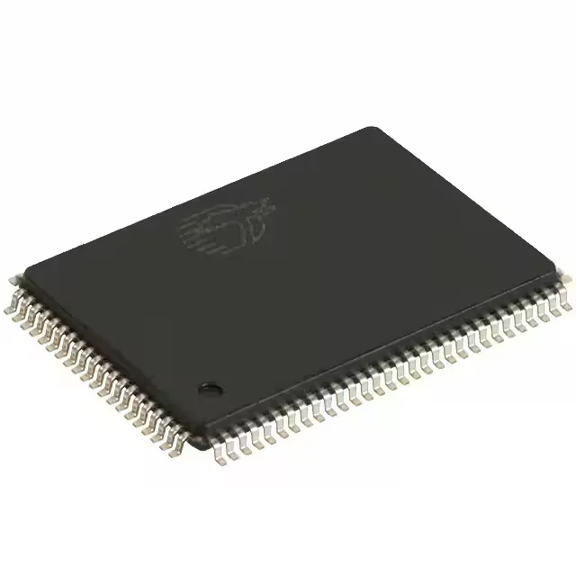
72Mbit NoBL synchronous SRAM for high-throughput data buffering
It runs on a 3.3V supply (3.135V to 3.6V range) and clocks at 167 MHz with a 3.4 ns access time, delivering back-to-back read/write transactions without dead cycles on the bus.
The 167 MHz clock rate and 3.4 ns access time are the headline specs that determine whether this part can keep up with a high-speed ASIC, FPGA, or network processor. The NoBL architecture eliminates the dead cycle that conventional synchronous SRAMs insert when switching between read and write — every clock edge can be a valid transaction. For a 4M x 18 configuration, that means a peak bandwidth of roughly 3 Gbit/s on the data bus. The 3.4 ns access time gives the controller about one clock cycle of setup margin at 167 MHz, so board-level signal integrity matters: keep trace lengths matched and place the termination resistors close to the memory pins.
Industrial temperature grade and 3.3V supply rail
The 3.135V to 3.6V supply window means the part runs comfortably on a nominal 3.3V rail with ±5% tolerance — typical for most digital systems. The 100-TQFP package has a 0.5 mm pitch and a 14x20 mm body; the exposed pad is not present on this package variant, so all thermal dissipation goes through the leads. Decouple with a 0.1 µF ceramic per supply pin pair, placed as close to the package as the board allows.