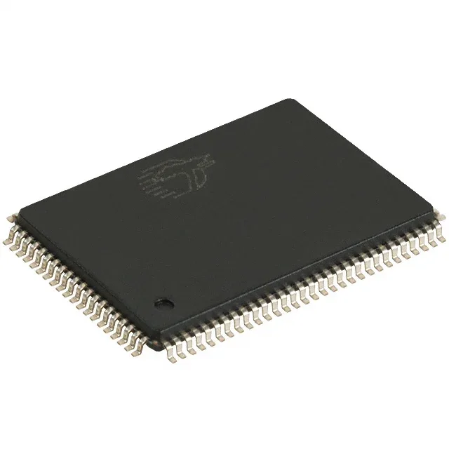
72 Mbit NoBL synchronous SRAM at 200 MHz
It clocks at 200 MHz with a 3 ns access time, meaning the memory can sustain a read or write on every clock cycle with zero dead cycles between transactions — a critical feature for high-throughput data buffers, look-up tables, and packet-processing engines in networking and telecom equipment.
200 MHz clock and 3 ns access — timing closure considerations
At 200 MHz the clock period is 5 ns, and with a 3 ns access time the output data is valid for about 2 ns of the cycle. That leaves a tight window for the controller to capture the read data, especially across temperature and voltage corners. The board layout needs controlled-impedance traces and matched-length routing between the SRAM and the FPGA or ASIC controller; a 100-TQFP package with its 0.5 mm pitch demands careful fanout and via placement to keep stub lengths short. The 2.5 V supply rail must be locally decoupled with low-ESR capacitors within 5 mm of each supply pin pair to maintain signal integrity at this speed.
NoBL architecture — what it changes in the bus protocol
Conventional pipelined synchronous SRAMs insert one dead cycle when switching from read to write or vice versa. The NoBL architecture eliminates that penalty: the controller can issue a read on cycle N and a write on cycle N+1 without an idle cycle in between. For a system doing mixed read-write traffic — a network switch buffer, for instance — this recovers up to 50% of the bus bandwidth that would otherwise be lost to turnaround cycles. The trade-off is that the controller must support the NoBL protocol (essentially a single-cycle command interface) rather than the older pipelined flow-through scheme.
Package and footprint — 100-TQFP (14x20 mm)
The CY7C1472V25-200AXC is supplied in a 100-lead TQFP with a 14x20 mm body and 0.5 mm pitch. It is a surface-mount package suitable for standard reflow assembly. The supplier device package designation is 100-TQFP (14x20). No exposed thermal pad is present on this package; heat dissipation relies on the leadframe and board copper, so the ambient temperature ceiling of 70°C must be respected in the system thermal design.
Lifecycle status — active, no end-of-life watch needed
No official replacement or successor is listed, which is expected for a current-production device.