Cypress Semiconductor lists the CY7C1472BV33-167BZC as obsolete.
The 167 MHz clock rate and 3.4 ns access time define the speed bin for this 72 Mbit synchronous SRAM. Running the part at a slower clock is fine, but the 167 MHz ceiling sets the upper bound for the system's read/write bandwidth.
72 Mbit organized 4M x 18 — memory map fit
The 72 Mbit density is organized as 4 million words of 18 bits each. The 18-bit word width (16 data bits plus 2 parity/ECC bits) is common in networking ASIC interfaces that use a 16-bit data bus with byte parity. The parallel memory interface requires a 4M-word address space from the controller. If your design uses a 32-bit or 36-bit data bus, two or four of these parts can be banked together with shared address and control lines.
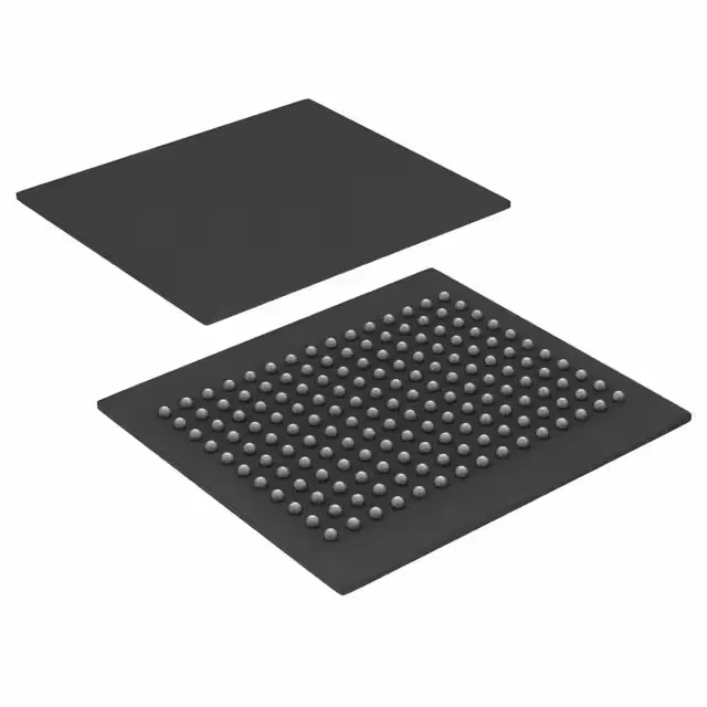
165-FBGA (15x17) — BGA rework considerations
The 165-ball FBGA package measures 15 mm x 17 mm. The surface-mount footprint must match the supplier device package code 165-FBGA (15x17); verify the PCB land pattern against the Cypress package drawing before committing the board.
Not suitable for outdoor base stations, industrial motor drives, or automotive applications where the ambient temperature exceeds 70°C or drops below freezing.
Supply voltage: 3.135V to 3.6V
The 3.3 V I/O level is compatible with most FPGA banks and ASIC memory controllers running at 3.3 V.