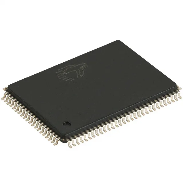
The CY7C1472BV25-200AXC is a 72Mbit synchronous SRAM from Infineon's NoBL (No Bus Latency) series, organized as 4M x 18. It clocks at 200 MHz with a 3 ns access time, eliminating the dead bus cycle between read and write operations typical of standard synchronous SRAMs. Supply voltage range is 2.375V to 2.625V — a narrow 2.5V core rail that demands a clean supply; a 1% LDO or a low-noise regulator ahead of the VDD pins is the usual call.
The 100-TQFP (14x20) supplier package footprint is standard — the 0.5 mm pitch means a 4-layer board is the practical minimum for fan-out; two-layer boards will struggle to route the 18-bit data bus plus address and control lines without vias stacking up. Supplied in tray packaging — typical for low-volume prototyping or manual assembly. For reflow, the LQFP body is moisture-sensitive; bake before reflow if the floor life has been exceeded.
Memory interface and timing
The parallel memory interface operates at 200 MHz with a 3 ns access time — the NoBL architecture means the next access can start on the clock edge immediately following a write, so the bus stays full. For a system running a 200 MHz bus clock, the 3 ns access fits within a single cycle with margin; the setup and hold times on the address and data lines will be the limiting factor, not the access window itself. Memory organization is 4M x 18 — 18-bit wide data bus, so it pairs naturally with a 16-bit or 18-bit processor bus. The extra two bits can serve as parity or ECC bits, or be left unused if the controller supports byte enables.