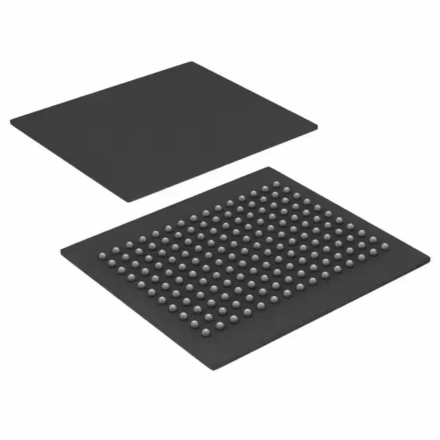
200 MHz NoBL synchronous SRAM — 72Mbit in 165-FBGA
The CY7C1470V33-200BZI is a 72Mbit synchronous SRAM from Infineon's NoBL (No Bus Latency) family, organized as 2M x 36 and clocked at 200 MHz. It delivers a 3 ns access time from clock edge, meaning the read data is available on the bus within three clock cycles at full speed — the NoBL pipeline eliminates the dead cycle between read and write transitions that conventional synchronous SRAMs require. The 165-ball FBGA package (15x17 mm body) routes 36 data lines plus address and control onto a single layer of the PCB — the fine-pitch BGA demands a controlled-impedance layout and at least four layers for signal integrity at 200 MHz.
Memory interface and board integration
The parallel memory interface uses a common address bus for read and write — the NoBL architecture lets the controller issue a read on one clock edge and a write on the next without inserting an idle cycle, sustaining full bus utilization at 200 MT/s. The 165-FBGA footprint is shared with other densities in the NoBL family, so a single PCB layout can accept 36Mbit, 72Mbit, or 144Mbit variants by changing the BOM line — useful for a single-board design that scales across product tiers.