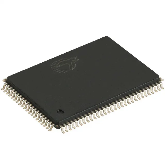
Infineon Technologies CY7C1470V33-200AXC — Memory (DRAM / SRAM / Flash / EEPROM)

CY7C1470V33-200AXC 72Mbit SRAM, 200 MHz, 3 ns, 100-LQFP

MPNCY7C1470V33-200AXC
Obsolete

Infineon Technologies NoBL™ CY7C1470V33-200AXC synchronous SDR SRAM, 72Mbit, 200 MHz clock, 3 ns access, 2M x 36 organization, 3.135V–3.6V supply, 100-LQFP tray, 0°C–70°C.

$148.8400Ref. price · indicative, final on quote
Independent supplier — new & surplus stockAuthenticity-screened · ESD-safe packingListing updated Jul 2026

Specifications

CY7C1470V33-200AXC specifications
ParameterValue
SeriesNoBL™
Memory typeVolatile
MountingSurface Mount
Supply voltage3.135V ~ 3.6V
Clock frequency200 MHz
Memory interfaceParallel
Operating temperature0°C ~ 70°C (TA)
PackageTray
TechnologySRAM - Synchronous, SDR
Access time3 ns
Memory size72Mbit
Memory formatSRAM
Case100-LQFP
Memory organization2M x 36

Product details

72Mbit synchronous SRAM with 200 MHz no-bus-latency pipeline

The Infineon CY7C1470V33-200AXC is a 72Mbit synchronous SDR SRAM from the NoBL™ series, organized as 2M x 36. It clocks at 200 MHz with a 3 ns access time, meaning the pipeline delivers a new data word every clock cycle without dead cycles between read and write turns — critical for high-throughput data buffers in networking or test equipment where bus-turnaround latency eats into throughput. The 3.135V–3.6V supply range and 0°C–70°C commercial temperature grade target indoor, controlled-environment gear — think base-station line cards, ATE pattern memory, or high-end FPGA configuration stores — not automotive or outdoor deployment.

Package, footprint, and reflow reality

Housed in a 100-LQFP (supplier device package 100-TQFP 14x20), this is a standard fine-pitch QFP with 0.5 mm lead pitch. The exposed pad is absent — no thermal-paste stencil step, no paddle solder joint to inspect. The 14x20 mm body sits on a standard footprint — no exotic pad geometry, no via-in-pad requirement. A single reflow profile for 0.5 mm pitch QFPs handles it; tombstoning risk is low because the leads are on all four sides and the part is symmetric.

No pin-compatible drop-in replacement from Infineon is documented; a board spin or parametric search for a 2M x 36 synchronous SRAM in a 100-pin QFP may yield alternatives from other vendors, but those are not cross-referenced here.

Frequently asked questions

What is the memory organization and interface of the CY7C1470V33-200AXC?

It is organized as 2M x 36 (72Mbit total) with a parallel synchronous interface. The 36-bit word width suits wide data buses in networking or DSP applications where a single chip covers a full 36-bit datapath.

What package does the CY7C1470V33-200AXC use and what is the reflow concern?

It comes in a 100-LQFP (100-TQFP 14x20) — a standard 0.5 mm pitch QFP. No exposed paddle. MSL is not on the record; assume MSL 3 and bake before reflow if the floor life is uncertain. Standard QFP reflow profile applies.