200 MHz NoBL synchronous SRAM — what the 3 ns access time buys you
It clocks at 200 MHz and delivers a 3 ns access time from address to data valid. The NoBL architecture eliminates the dead cycle when the bus switches from read to write, so back-to-back transactions sustain full 200 MHz throughput without a turnaround penalty. That matters in packet-forwarding engines, network switches, and DSP pipelines where every bus cycle counts.
2.5 V supply — verify your memory bus voltage
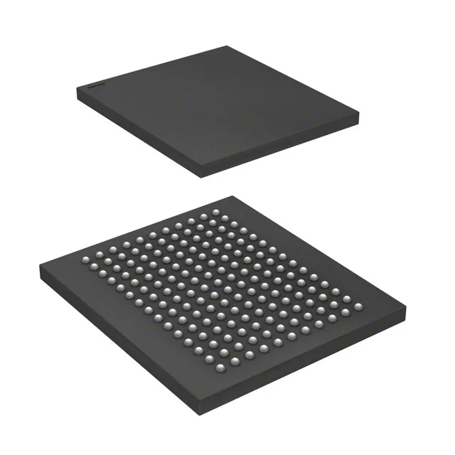
The supply range is 2.375 V to 2.625 V, nominally 2.5 V. If you are replacing a 3.3 V synchronous SRAM on an existing board, the voltage mismatch means a separate 2.5 V plane or a regulator change. The 165-FBGA (15x17) footprint is a fine-pitch BGA — route the 2.5 V plane with enough copper for the transient current draw at 200 MHz.
Industrial temperature grade — -40 to 85°C
The 200 MHz clock and 3 ns access time hold across the full temperature range, but timing margin shrinks at the hot end — budget for derating in the signal-integrity simulation.