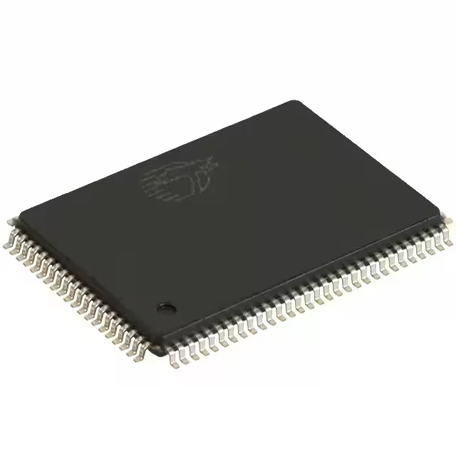
72 Mbit NoBL SRAM for high-throughput datapaths
The CY7C1470V25-200AXC: Clocked at 200 MHz with a 3 ns access time, this part targets high-bandwidth applications like network packet buffers, telecom line cards, and test equipment where back-to-back transactions without turnaround penalty are essential. It operates from a 2.375 V to 2.625 V supply and is housed in a 100-TQFP (14x20 mm) package suited for surface-mount assembly.
200 MHz clock, 3 ns access — timing margin in practice
At 200 MHz the clock period is 5 ns. With a 3 ns access time from clock edge to data valid, the part leaves roughly 2 ns for board trace delay and receiver setup — tight but workable with proper signal-integrity layout. The 36-bit-wide data bus can be paired with a second device for 72-bit ECC protected memory, common in router forwarding tables. The synchronous SDR interface means all control signals (address, chip select, write enable) are sampled on the rising clock edge, simplifying timing closure in an FPGA or ASIC controller.
Supply and temperature — indoor systems only
The 2.375 V to 2.625 V supply is a narrow 2.5 V nominal rail; a 1.8 V or 3.3 V system needs an extra regulator. Not rated for outdoor, industrial, or automotive use where -40°C to 85°C or wider is required.
Infineon lists the CY7C1470V25-200AXC as Active. The base product number CY7C1470 covers multiple speed and temperature variants; the -200AXC suffix specifies the 200 MHz speed grade in the commercial temperature TQFP package.