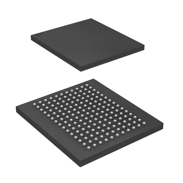
The CY7C1470BV33-200BZCT: The NoBL architecture eliminates the dead bus cycles typical of pipelined SRAMs during read-to-write or write-to-read transitions, sustaining full back-to-back throughput at the rated clock rate. It is designed for high-bandwidth cache buffers, network packet memory, and DSP scratchpad applications where deterministic latency and continuous data flow are required.
200 MHz clock and 3 ns access — what the timing means for the bus
The 200 MHz clock frequency and 3 ns access time are the headline timing specs. At 200 MHz, the cycle time is 5 ns, and the 3 ns access time leaves a 2 ns window for address-to-data valid plus hold — tight but workable with a well-terminated PCB layout. The NoBL pipeline means the part can accept a new read or write address every clock cycle without inserting idle cycles for bus turnaround, which is the key advantage over standard synchronous SRAMs. For a design already using a 3.3 V SRAM bus at 133 MHz or 166 MHz, this part offers a direct speed upgrade path without changing the supply rail or memory organization.
Obsolete — lifecycle reality and sourcing path
The CY7C1470BV33-200BZCT is officially marked as Obsolete by Cypress (now Infineon).
The ball pitch and layout follow the standard Cypress 165-ball FBGA footprint for this density tier. For PCB layout, confirm the ball-out against the datasheet — the 2M x 36 organization maps to 36 data lines plus address, control, and clock signals.