Infineon Technologies CY7C1470BV33-200BZC — Memory (DRAM / SRAM / Flash / EEPROM)

CY7C1470BV33-200BZC NoBL SRAM, 72Mbit, 200 MHz, 165-FBGA

MPNCY7C1470BV33-200BZC
Obsolete

Infineon Technologies NoBL™ Synchronous SRAM, 72Mbit, 2M x 36 organization, 200 MHz clock, 3 ns access time, 3.135V–3.6V supply, 165-FBGA (15x17), Tray.

$127.9900Ref. price · indicative, final on quote
Independent supplier — new & surplus stockAuthenticity-screened · ESD-safe packingListing updated Jul 2026

Specifications

CY7C1470BV33-200BZC specifications
ParameterValue
SeriesNoBL™
Memory typeVolatile
MountingSurface Mount
Supply voltage3.135V ~ 3.6V
Clock frequency200 MHz
Memory interfaceParallel
Operating temperature0°C~70°C(TA)
PackageTray
TechnologySRAM - Synchronous, SDR
Access time3 ns
Memory size72Mbit
Memory formatSRAM
Case165-LBGA
Memory organization2M x 36

Product details

72Mbit NoBL synchronous SRAM — 200 MHz pipeline

The CY7C1470BV33-200BZC is a 72 Mbit synchronous SRAM organized as 2M x 36, built on Infineon's NoBL (No Bus Latency) architecture. It clocks at 200 MHz with a 3 ns access time from the clock edge, meaning the read data appears on the bus within one clock cycle of the address — no dead cycles between read and write turns. This is a volatile, SDR (single data rate) SRAM with a parallel memory interface, supplied from a 3.135 V to 3.6 V rail.

Package and board-fit — 165-ball FBGA

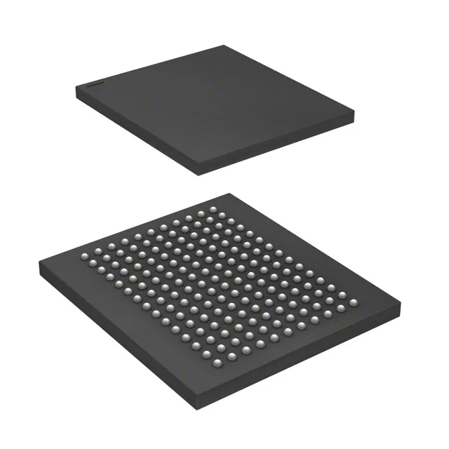
Housed in a 165-ball LBGA (supplier device package 165-FBGA, 15x17 mm), this is a fine-pitch BGA that requires a multilayer PCB for fan-out.

Frequently asked questions

What is the memory organization of CY7C1470BV33-200BZC?

2M x 36 — 2,097,152 words of 36 bits each, for a total of 72 Mbit. The 36-bit word width suits systems with 32-bit data plus parity or ECC overhead.

What package does CY7C1470BV33-200BZC use?

165-ball LBGA (low-profile ball grid array), supplier device package 165-FBGA with a 15x17 mm body. The balls are on a 1.0 mm pitch.

What supply voltage does CY7C1470BV33-200BZC require?

3.135 V to 3.6 V, with a nominal 3.3 V rail. All I/O are 3.3 V tolerant — no level translation needed when interfacing to a 3.3 V controller or FPGA bank.

What is the clock frequency and access time?

200 MHz maximum clock frequency. The access time from the rising clock edge is 3 ns — the data is valid on the bus within one cycle of the address being registered.