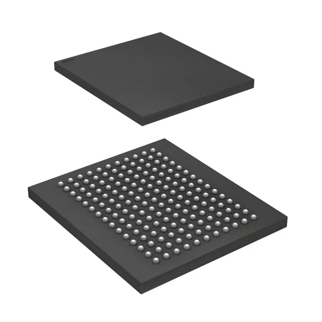
Active production — 250 MHz synchronous SRAM in 165-FBGA
The CY7C1470BV25-250BZXC is an Infineon NoBL™ 72Mbit synchronous SRAM with a 250 MHz clock and a 3 ns access time, organized as 2M x 36.
Clock speed and access time — timing closure drivers
The 250 MHz clock rate sets the peak data bandwidth at 1 GB/s on a 36-bit bus. The 3 ns access time is the latency from address to data valid — at this speed, board trace length and signal integrity on the parallel interface become the limiting factors, not the SRAM itself. Operating from a 2.375V to 2.625V supply, the part is a pure 2.5 V device — do not mix with 3.3 V I/O without a level translator.
165-FBGA package — rework and layout considerations
The 165-FBGA (15x17 mm) package is a fine-pitch BGA. From a rework standpoint, this part will survive hot-air removal if the board is pre-baked per J-STD-033 for moisture sensitivity — skip the bake and the internal delamination risk goes up. The 0.8 mm ball pitch is hand-reworkable with a stencil and a decent reflow station, but the 165 balls mean you need a bottom-side preheater to avoid warping the board. For PCB layout, the 15x17 mm footprint requires a 4-layer board minimum to fan out the inner rows. Place decoupling capacitors (0.1 µF and 1 µF) within 5 mm of each supply ball pair — the 250 MHz switching current demands low-inductance paths.
Sourcing — active, available per RFQ
Lifecycle status is Active — Infineon has not issued a PCN or end-of-life notice for this order code. Confirm the specific date-code and packaging (tray) with your quote request.