200 MHz synchronous SRAM with NoBL™ — what the 3 ns access means for your bus
The CY7C1470BV25-200BZI is a 72 Mbit synchronous SRAM organized as 2M x 36, clocked at 200 MHz with a 3 ns access time. The NoBL™ (No Bus Latency) architecture eliminates the dead cycle normally required when the bus turns from read to write on the same bank — the next command can issue on the very next clock edge. For a packet buffer or cache line that alternates read and write accesses, this means sustained throughput at the full 200 MHz rate rather than the 100 MT/s effective rate of a traditional pipelined SRAM.
Supply rail and temperature — 2.5V core, industrial range
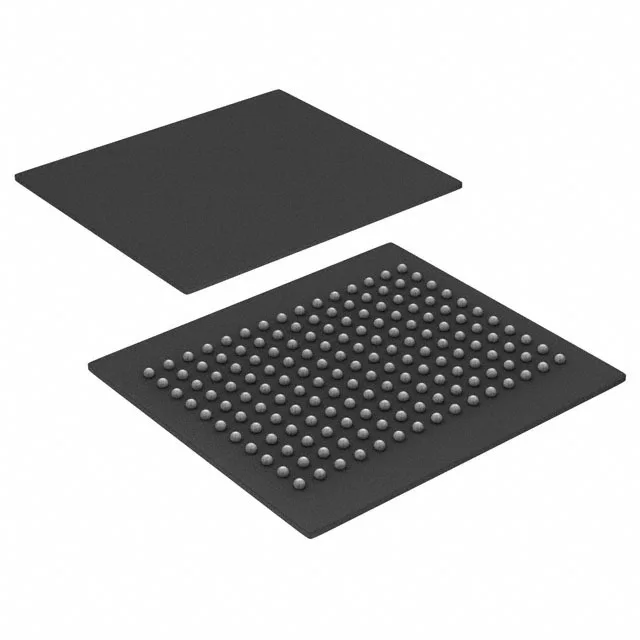
The supply range is 2.375V to 2.625V — a nominal 2.5V rail. It will not run from a 1.8V or 3.3V supply without an intermediate regulator. The 165-FBGA (15x17 mm) package is a fine-pitch BGA. MSL rating is not in the record, but a 0.8 mm or 1.0 mm ball pitch is typical for this package class — the reflow profile must match the solder paste alloy, and X-ray inspection is needed to detect head-in-pillow or voiding under the BGA.
Obsolete — sourcing reality for the CY7C1470BV25-200BZI
New production has ended; the only supply channel is independent surplus and broker inventory. Each lot is date-code and quantity-specific — confirmed at RFQ. No pin-compatible drop-in replacement is listed, so a board spin or a parametric search for a 2.5V, 200 MHz, 72 Mbit synchronous SRAM in a 165-ball FBGA is the migration path for new designs.