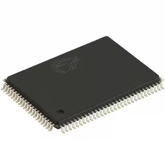
72 Mbit at 200 MHz — the NoBL architecture decision
The CY7C1470BV25-200AXC is a 72 Mbit synchronous SRAM organized 2M x 36, clocked at 200 MHz with a 3 ns access time. It belongs to the NoBL (No Bus Latency) family, which eliminates the dead cycle between read and write operations — the bus switches direction without an idle clock, so a mixed read/write transaction sequence sustains full throughput without pipeline bubbles. This matters for high-bandwidth data buffers in network switches, base stations, or test equipment where the memory controller must interleave reads and writes on the same port without stalling the pipeline. At 200 MHz, the 36-bit data bus delivers 900 MB/s peak bandwidth, and the NoBL flow keeps that figure real under mixed traffic.
Supply rail and temperature envelope
The device operates from a 2.375 V to 2.625 V supply — a tight 2.5 V ±5 % rail. Packaged in a 100-LQFP (supplier device package 100-TQFP, 14x20 mm), the 0.5 mm pitch footprint is standard for high-pin-count synchronous SRAM. The tray delivery suits medium-to-high volume pick-and-place; the part is not supplied on tape-and-reel in this order code variant.
Active lifecycle — no LTB pressure, but watch the allocation window
Infineon lists the CY7C1470BV25-200AXC as Active. That means the part is still in the standard production portfolio and can be ordered through franchised distribution without an end-of-life clock running. That said, synchronous SRAM is a mature product category. Lead times can stretch during allocation cycles when foundry capacity shifts to higher-volume logic or memory types.
The part carries the Infineon brand mark and is supplied in original manufacturer packaging (tray).