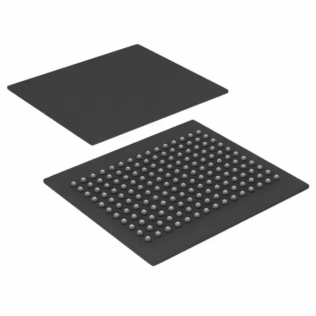
36 Mbit NoBL synchronous SRAM for high-throughput pipelines
It clocks at 167 MHz and delivers a 3.4 ns access time, which means the memory can sustain back-to-back read/write operations without dead cycles on the bus — a requirement for high-throughput data buffers in network switches, base station line cards, and telecom infrastructure where every clock cycle counts.
167 MHz clock and 3.4 ns access — what they mean for timing closure
A 167 MHz clock period is roughly 6 ns. With a 3.4 ns access time, the SRAM leaves about 2.6 ns of setup/hold margin for the controller or FPGA I/O at the rated frequency — enough for most 2.5V-class interfaces, but tight enough that you'll want to verify the input timing budget against your specific controller's data sheet. The NoBL architecture eliminates the turnaround cycle when switching from read to write, so the effective throughput at 167 MHz is closer to a pipelined burst than a conventional synchronous SRAM. If your design runs a 133 MHz or slower bus, the margin improves proportionally.
165-ball FBGA — rework and layout notes
The package is a 165-ball FBGA with a 15x17 mm body. The ball pitch is 1.0 mm (standard for this density), which is hand-reworkable with a good hot-air station and a stencil — but the 15x17 mm footprint has significant thermal mass, so preheat the board to 100-110°C before attempting removal. Orientation is marked by a chamfered corner on the substrate; verify pin A1 location against the datasheet's ball-map diagram before placing. The part is MSL 3 per Cypress standard for this package family — bake at 125°C for 48 hours if the moisture-barrier bag has been open longer than the floor-life window.