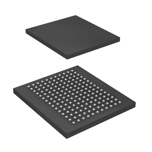
Infineon Technologies CY7C1460AV25-200BZI — Memory (DRAM / SRAM / Flash / EEPROM)

CY7C1460AV25-200BZI Infineon NoBL SRAM, 36Mbit, 200 MHz

MPNCY7C1460AV25-200BZI
Obsolete

Infineon (Cypress) NoBL 36Mbit synchronous SRAM, 200 MHz clock, 3.2 ns access, 2.5V supply, 165-FBGA, -40 to 85°C operating temperature, CY7C1460AV25-200BZI.

$57.7000Ref. price · indicative, final on quote
Independent supplier — new & surplus stockAuthenticity-screened · ESD-safe packingListing updated Jul 2026

Specifications

CY7C1460AV25-200BZI specifications
ParameterValue
SeriesNoBL™
Memory typeVolatile
MountingSurface Mount
Supply voltage2.375V ~ 2.625V
Clock frequency200 MHz
Memory interfaceParallel
Operating temperature-40°C~85°C(TA)
PackageTray
TechnologySRAM - Synchronous, SDR
Access time3.2 ns
Memory size36Mbit
Memory formatSRAM
Case165-LBGA
Memory organization1M x 36

Product details

It delivers a 200 MHz clock rate and a 3.2 ns access time, operating from a 2.375 V to 2.625 V supply. The NoBL architecture eliminates dead cycles between read and write turns, sustaining full back-to-back throughput — a key advantage in high-bandwidth data paths like network packet buffers, DSP lookup tables, or FPGA cache memory.

A 3.2 ns access time at 200 MHz means the part can deliver data within one clock cycle from the address, with zero wait states on a properly laid-out bus. This is the tier that keeps a 200 MHz FPGA or network processor fed without inserting pipeline bubbles. The parallel interface is 36 bits wide, so a single chip handles a full-word read or write per clock cycle. For designs that need sustained throughput on a wide data bus, this part eliminates the bus-turnaround penalty that standard synchronous SRAMs incur.

If your design is still in the prototype phase, consider qualifying a current-production synchronous SRAM in a compatible package and speed grade to avoid a future last-time-buy scramble.

The 0.8 mm ball pitch is reworkable with a hot-air station if you have a stencil and preforms, but the board needs a solder mask defined pad layout and via-in-pad with tenting on the back side.

Frequently asked questions

Is CY7C1460AV25-200BZI obsolete?

Yes, the CY7C1460AV25-200BZI carries an Obsolete lifecycle status. Infineon no longer manufactures this exact order code, and no official replacement part is listed in the record. Procurement must source from surplus or broker inventory.

What is the difference between CY7C1460AV25-200BZI and CY7C1460AV25-167BZI?

The primary difference is the clock speed: the -200BZI runs at 200 MHz with a 3.2 ns access time, while the -167BZI runs at 167 MHz with a correspondingly longer access time. Both share the same 36 Mbit density, 1M x 36 organization, 2.5 V supply range, and 165-FBGA package. The -200 variant is the higher-performance tier for designs that need the extra bus bandwidth.

What is the access time of CY7C1460AV25-200BZI?

The access time is 3.2 ns at the 200 MHz clock rate. This allows zero-wait-state reads and writes on a properly matched bus, sustaining full back-to-back throughput without dead cycles.

Can I replace CY7C1460AV25-200BZI with a non-obsolete part?

No official replacement is listed in the record. For a new design, consider a current-production synchronous SRAM from the same NoBL family or a compatible 36 Mbit, 200 MHz, 2.5 V, 165-FBGA part from another vendor. Pin compatibility and timing must be verified against the datasheet before substitution.