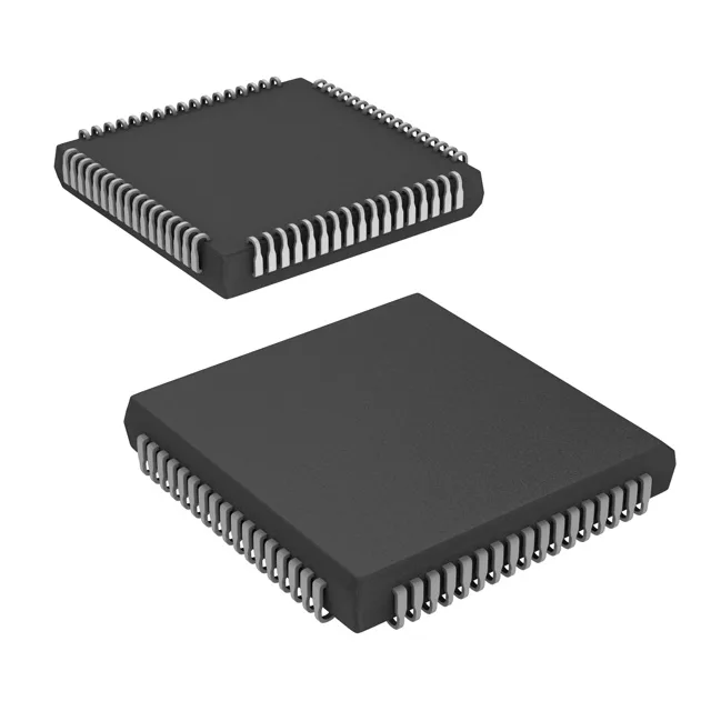
What this dual-port SRAM does on the board
Its defining feature is two independent ports with separate address, data, and control lines, allowing two bus masters — two processors, a processor and a DMA controller, or a processor and an FPGA — to read from or write to any memory location simultaneously.
55 ns access time means the SRAM presents valid data on the bus within 55 ns of the address and chip-enable signals settling.
The 68-lead PLCC with J-leads (24.23 mm x 24.23 mm body) is a surface-mount package that sits in a socket or solders directly to the board. J-leads are forgiving for hand rework compared to QFP gull-wing leads.
Obsolete — the sourcing picture
No further factory orders are being accepted; no last-time-buy window remains open.