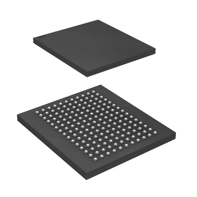
The Infineon CY7C1441AV25-133BZXI is a 36 Mbit synchronous single-data-rate (SDR) SRAM organized as 1M x 36, clocked at 133 MHz with a 6.5 ns access time. This part is designed for high-bandwidth buffer and cache applications in networking, telecom, and industrial control systems where deterministic read/write latency matters — think packet buffers, line cards, or FPGA co-processing memory. The 36-bit-wide data bus maps naturally to 32-bit processors plus parity or ECC overhead without external muxing.
133 MHz clock and 6.5 ns access — the timing budget
The 133 MHz clock frequency sets the bus cycle at 7.5 ns, and the 6.5 ns access time leaves about 1 ns of setup margin on a typical 133 MHz interface. That is tight — board trace length matching and signal integrity on the 36-bit parallel bus become critical. The synchronous pipeline eliminates the dead cycles of asynchronous SRAM, so back-to-back reads at full clock rate are possible. If your controller's timing closure budget is marginal at 133 MHz, this part will force a PCB respin; a slower 100 MHz variant in the same family might be the safer choice for legacy designs.
The 165-ball FBGA (15 x 17 mm) is a fine-pitch BGA — 1.0 mm ball pitch typical for this density. Reflow profile needs a ramp rate under 2°C/s to avoid head-in-pillow defects on the larger array.
Infineon lists the CY7C1441AV25-133BZXI as Obsolete.