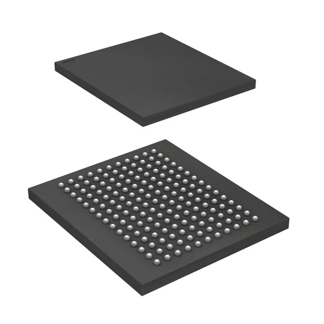
36Mbit synchronous SRAM for high-throughput data paths
Designed for high-bandwidth applications such as network switches, base stations, and telecom line cards, it delivers a 2.6 ns access time and supports a 250 MHz clock frequency, enabling pipelined read and write operations with minimal bus turnaround overhead.
2.6 ns access time and 250 MHz clock — timing closure for the bus
In a 250 MHz system with a 4 ns clock period, the 2.6 ns leaves roughly 1.4 ns for clock-to-output skew, board trace delay, and setup time at the receiving logic. This tight timing budget demands careful signal-integrity simulation and matched-length routing on the data and address buses — a point often missed when swapping in a slower-grade SRAM. The 250 MHz clock frequency supports back-to-back read/write transactions without dead cycles, critical for high-throughput packet processing in networking equipment. The synchronous interface simplifies controller design by eliminating the asynchronous handshake overhead.
Industrial temperature and FBGA package — deployment context
For production runs that already have this SRAM in the BOM, the only reliable channel is independent distribution — verified date-code lots, sourced against an RFQ. The FBGA package and 2.5V supply rail are not drop-in compatible with the more common 3.3V synchronous SRAMs, so a board redesign is required if a substitute is needed. When sourcing obsolete BGA memory, date-code provenance matters: lots manufactured within two years of the last-time-buy date are preferable, as moisture sensitivity and solder-ball oxidation degrade over time. We quote each RFQ against current available stock, confirming the date code and quantity before committing the BOM line.