267 MHz DDR II — what the clock rate means for your bus
The CY7C1423AV18-267BZC is a 36 Mbit synchronous DDR II SRAM clocked at 267 MHz. Double-data-rate means data transfers on both clock edges, so the effective data rate is 534 MT/s per I/O — this keeps the memory bus matched to a high-throughput processor or ASIC without wait states. Organised 2M x 18, the wide-word architecture suits applications needing deep buffering with a narrow address bus — think network packet buffers, test equipment capture memory, or DSP coefficient storage.
Obsolete — sourcing reality for this SRAM
Infineon lists the CY7C1423AV18-267BZC as Obsolete. No pin-compatible drop-in replacement is documented by Infineon; a board-level redesign would be needed to migrate to a different SRAM family.
Package and supply — board-fit constraints
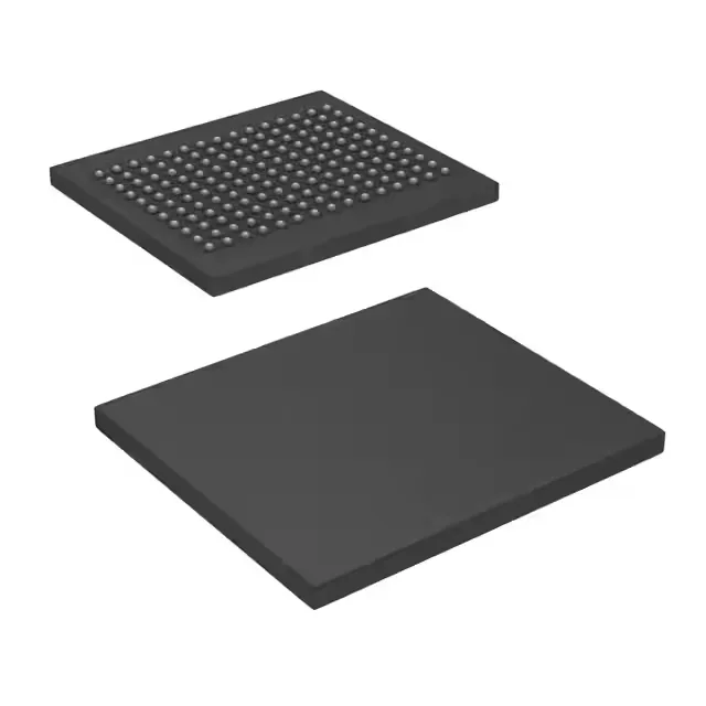
Housed in a 165-ball FBGA (15x17 mm). This is a fine-pitch BGA — not a hand-solderable package. The board requires a solder-paste stencil, reflow profile, and X-ray inspection for voiding. The 1.7 V to 1.9 V core supply needs a tight-regulation rail; a standard 1.8 V LDO with ±3% tolerance keeps the die within spec. Commercial temperature range: 0°C to 70°C. This limits deployment to indoor, climate-controlled equipment — no extended-temp or automotive use without active thermal management.