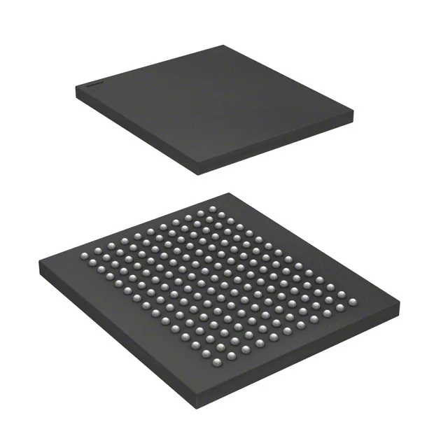
36 Mbit DDR II SRAM — what the 250 MHz clock buys you
The 250 MHz clock rate means the part can sustain a 500 MHz data rate on the bus, which directly determines the memory bandwidth available to an FPGA or ASIC in a line-rate application.
Infineon lists the CY7C1418BV18-250BZXC as Obsolete. For a production BOM that still calls out this exact density and speed grade, the path is either a last-time-buy from remaining distributor stock or a qualified second source through the independent channel. If your design can tolerate a different density or package variant within the CY7C1418 family, a pin-compatible drop-in may exist — but that requires a cross-reference against the specific footprint and timing budget. For new designs, look at current-generation DDR II+ or QDR SRAMs from the same vendor; the 165-FBGA footprint is common across several densities, so a layout-compatible upgrade is possible with a BOM change.
165-FBGA footprint and rework considerations
Supply voltage is 1.7V to 1.9V, so the board needs a dedicated 1.8V rail with tight regulation — a standard 1.8V LDO or switcher, but the tolerance window is narrow enough that a 1.8V ±5% supply is marginal at the low end.