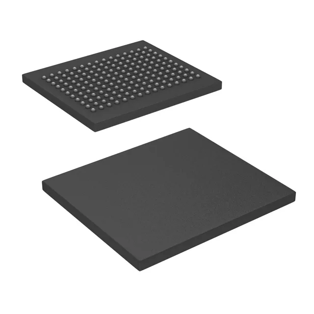
The Cypress CY7C1415AV18-167BZC is a 36Mbit synchronous SRAM built on the QDR II architecture — separate read and write data ports running at 167 MHz, organized as 1M x 36. That dual-port structure eliminates bus-turnaround dead cycles, so a network processor or ASIC can push a read and a write in the same clock cycle. It's the kind of memory you find in packet buffers, traffic managers, and high-end test equipment where back-to-back throughput matters more than density. The 1.7V to 1.9V supply range puts it on a nominal 1.8V rail, and the 165-FBGA package (15x17mm) keeps the signal paths short for the 167 MHz interface.
At 167 MHz, each port delivers a 36-bit word every cycle, so the aggregate bandwidth is roughly 12 Gbps across the two ports. That's the number that matters when you're sizing the memory subsystem for a 10G line card or a logic analyzer acquisition buffer. The QDR II interface is source-synchronous with echo clocks — the SRAM sends back a delayed version of the input clock to simplify the data capture window. Layout needs matched trace lengths on the 36-bit data buses and the clock pair; the 165-FBGA ball map is designed to keep that manageable on a 6- or 8-layer board.
If you're qualifying a new design, look at the active QDR II+ or QDR IV generations from Cypress (now Infineon) for a forward-compatible road map, but expect a different package and supply voltage.
Package and temperature — the board-level realities
The 165-FBGA (15x17mm) is a 1.0 mm ball-pitch BGA.