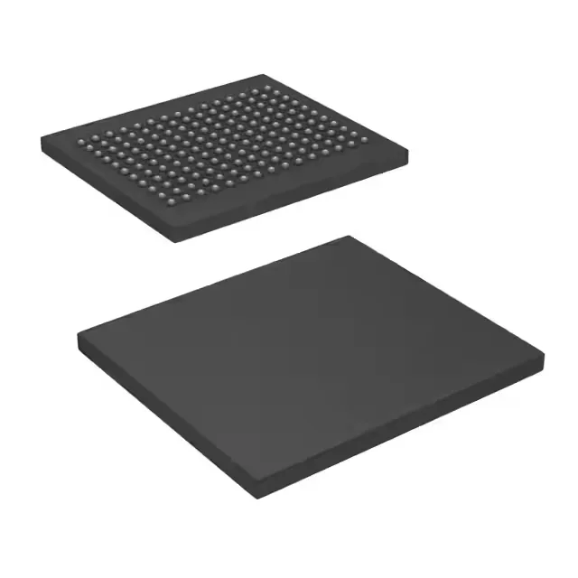
36Mbit QDR II SRAM — what the 300 MHz clock buys you
The CY7C1413JV18-300BZXC is a 36 Mbit Quad Data Rate II synchronous SRAM organized as 2M x 18 bits, clocked at 300 MHz. QDR II architecture transfers data on both rising and falling edges of the clock, delivering a 600 MHz effective data rate on the read and write ports simultaneously — purpose-built for high-throughput buffer applications in networking line cards, telecom switches, and test equipment where latency matters more than density. The parallel memory interface and 1.7 V to 1.9 V supply rail mean this part integrates into a dedicated memory bus, not a serial SPI or I2C chain — the board already carries a QDR II controller and the appropriate supply regulator.
Obsolete — sourcing reality for the BOM line
The 165-FBGA (15x17 mm) footprint is fixed — any pin-compatible replacement would need to share the same ball map and supply voltage. Without an official cross-reference from Infineon, a board spin is the only guaranteed migration path if the original part cannot be sourced.
Housed in a 165-ball LBGA (15x17 mm FBGA), surface-mount only. Supplied in tray packaging, not tape-and-reel — this affects pick-and-place feeder setup for volume assembly. Confirm the tray count per reel equivalent with your contract manufacturer before committing to a production run.