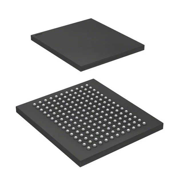
It is organized as 2M x 18 and clocks at 250 MHz, delivering back-to-back read and write transactions on every clock edge without dead cycles — the hallmark of the QDR II bus. This part is designed for high-throughput buffer applications where the bus must sustain full-rate reads and writes simultaneously: network switches, line cards, telecom line cards, and high-end test equipment that demand deterministic latency and zero bus-turnaround penalty.
At 250 MHz the QDR II interface delivers a peak bandwidth of 1 GB/s per port (18-bit data bus, DDR on both read and write ports). That tighter voltage window demands a clean, low-noise 1.8 V supply with ±5% regulation.
Infineon (formerly Cypress) has ended production on this QDR II density and speed grade. The 165-ball FBGA package (15x17 mm) means any substitute would need to match the same footprint and ball map to avoid a PCB re-spin.
Package and board-level handling
The fine-pitch BGA needs X-ray inspection after reflow to verify ball wetting and voiding.