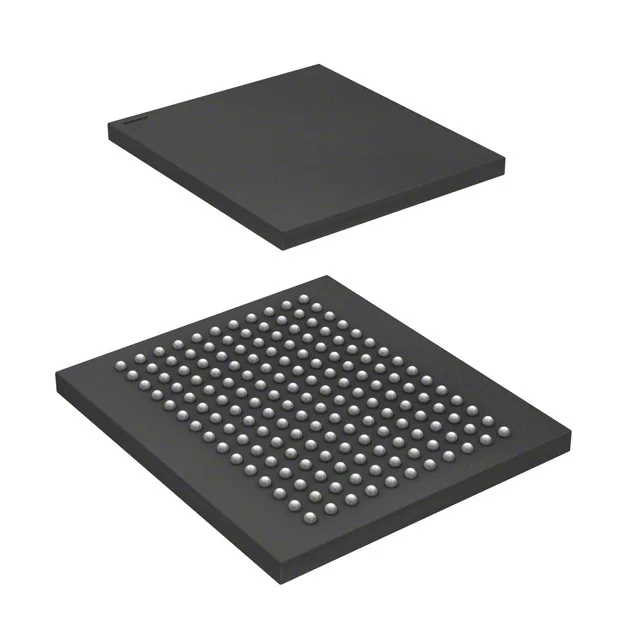
It is designed for high-bandwidth, low-latency buffer applications where a dedicated read and write port eliminates bus-turnaround dead cycles. Typical deployment includes network switch buffers, line-card packet memory, and high-end test equipment that needs sustained throughput at a 200 MHz clock rate.
The 200 MHz clock drives a QDR-II interface that delivers two data words per clock cycle on both read and write ports, yielding a peak bandwidth of 7.2 Gbps (200 MHz × 18 bits × 2). This matters for designs that must move large blocks of data without stalling the processor or ASIC. The 1.7–1.9 V core supply keeps I/O levels compatible with low-voltage logic families, but the 0–70 °C commercial temperature range limits use to controlled indoor environments — not industrial or automotive.
The 165-LBGA footprint (15×17 mm body) is shared with other QDR-II density variants in the CY7C1412 family, but pin compatibility across the family should be verified against the respective datasheets.