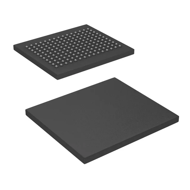
QDR II means the part reads and writes on both clock edges, effectively doubling the data rate without increasing the clock frequency — useful in high-throughput buffer applications like network switches, telecom line cards, and test equipment where back-to-back read-write cycles with zero dead cycles are required.
At 167 MHz, the QDR II interface delivers a peak bandwidth of 333 million transfers per second per 18-bit port (read and write each get their own port). That translates to roughly 6 Gbps of raw I/O bandwidth across the two ports. For a system designer, the key takeaway is that the bus timing margin at this speed is tight — the 1.7–1.9 V supply needs to be clean and within 3% of the target, and the PCB trace length matching between the address/control and data buses should be held to within 50 ps of skew to avoid setup/hold violations. This is not a part you drop into a noisy 1.8 V rail shared with a switching regulator without a pi-filter.
Cypress (now part of Infineon) no longer manufactures it, and no official successor part number has been recorded. If you are designing a new board, do not plan this part in; look at current-generation QDR II+ or QDR IV parts from Infineon or Renesas for a drop-in or near-drop-in alternative.
Package and board integration notes
It is surface-mount only, and the 1.7–1.9 V core supply means the board needs a dedicated 1.8 V rail — do not share it with 1.8 V I/O banks on an FPGA that might draw transient current spikes.