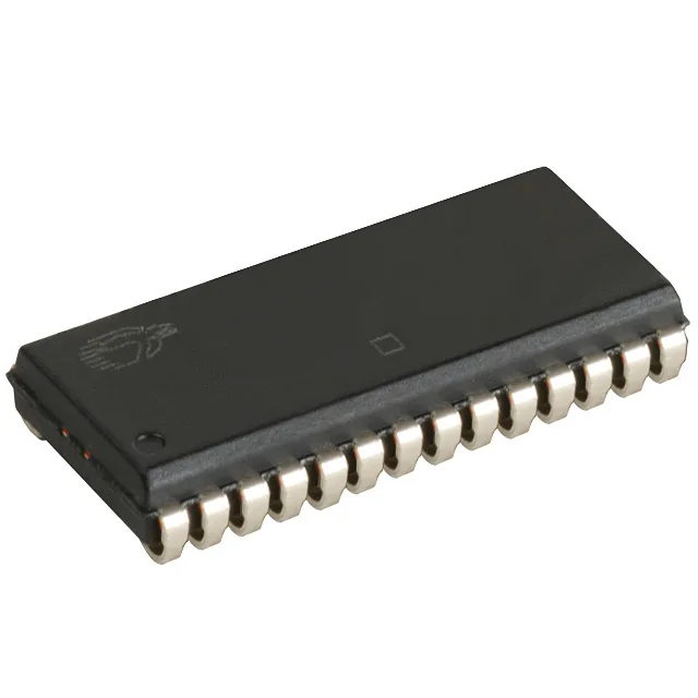
15 ns access time and bus timing
The CY7C1399B-15VXC: The 15 ns access time means the SRAM presents valid data on the bus within 15 ns of the address being stable — this sets the read-cycle timing margin for the memory controller or FPGA interface. Write cycle time is also 15 ns, so the part can complete a full read or write operation in a single 66 MHz clock cycle with zero wait states, provided the controller's output hold time is met.
SOJ package — rework and board-fit
The 28-SOJ package (JEDEC MO-061, 300 mil body) has gull-wing leads on a 1.27 mm pitch — it is hand-solderable with a fine-tip iron and reworkable under hot air without lifting pads, unlike finer-pitch QFPs.
Obsolete — sourcing reality
No pin-compatible direct replacement exists from Infineon — a functional equivalent would require a different package or speed grade, and a board spin may be needed.